U.S.–Japanese Consortium "US-JOINT" Begins Full-Scale Development of Next-Generation Semiconductor Packages
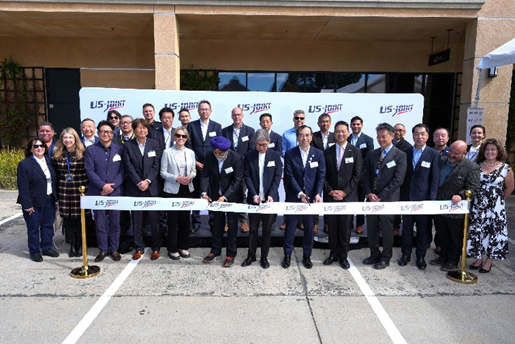
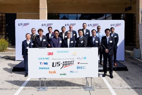
Union City, CA, USA (April 20, 2026) TOKYO OHKA KOGYO CO., LTD. (Headquarters: Kawasaki, Japan/ President: Noriaki Taneichi, hereinafter the “Company”) today announced the establishment of a new R&D center to mark the full-scale launch of “US-JOINT,” a consortium comprising 12 Japanese and U.S. materials and equipment manufacturers, with the goal of establishing new models for developing next-generation semiconductor-packaging technologies. To commemorate the occasion, a ceremony attended by government officials and participating companies from both countries was held at the consortium's newly operational base in Silicon Valley on April 20.
The new R&D center is the first in the United States dedicated to developing advanced semiconductor-packaging technologies. The consortium will leverage this R&D base in Silicon Valley to validate new concepts in collaboration with major users of advanced semiconductors. By capturing market needs in real time and combining the technological capabilities of leading Japanese and U.S. manufacturers of materials and equipment, the consortium will accelerate the research and development of materials, evaluation and packaging technologies to enable the rapid commercialization and deployment.
Overview of US-JOINT
|
Name |
US-JOINT (JOINT: Jisso Open Innovation Network of Tops) |
| Objectives |
To create an evaluation platform for next-generation semiconductor packaging and develop packaging technology in the United States. |
|
Participants (alphabetical order) |
12 companies (as of April 20, 2026) |
|
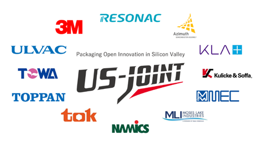
Resonac Corporation; Azimuth Industrial; KLA Corporation; Kulicke and Soffa Industries; MEC Co., Ltd.; Moses Lake Industries; Namics Corporation; Tokyo Ohka Kogyo Co., Ltd.; Toppan Inc.; TOWA Corporation; ULVAC, Inc.; and The 3M Company |
|
|
Location |
Union City, California, USA |
|
Launch |
April 2026 (full-scale operation) |
|
Main Facilities/Environment |
Advanced semiconductor packaging processes (patterning, bonding, molding, plating, etc.), evaluation and analysis equipment, cleanrooms (Classes 100 and 1,000). |
|
Facility Role |
R&D center for validating next-generation semiconductor-packaging concepts. |
|
Intended Users |
Fabless companies, semiconductor manufacturers, and engineers from participating companies. |
TOKYO OHKA KOGYO CO., LTD.’s Role in US-JOINT
Since our successful development of photoresists for semiconductors in 1968—the first of its kind in Japan—our company has led the industry in advancing semiconductor technology. We have consistently contributed to the realization of a prosperous and sustainable society.
At US-JOINT, we leverage the world-class microfabrication and ultra-high-purity technologies we have cultivated since our founding to advance the evolution of next-generation semiconductors. Through our high-performance, high-purity photoresists and related products, we continue to create value while contributing to a sustainable future through chemistry.
# # #
For Contact: Public Relations and IR Department
Tel. +81-44-435-3000