Semiconductor Manufacturing Field
Various chemicals, including photoresists that are a core product of the TOK, are used in the process of forming transistors and fine wiring inside semiconductor chips.
Semiconductor manufacturing flow
Front-end processes
- Photoresist coating
- Exposure
- Development
- Etching
- Photoresist cleaning
- Formation of a semiconductor field
- Formation of insulation film
- Formation of integra ted circuits
- Completion of an integrated circuit
- Development
- Etching
- Photoresist cleaning
- Formation of wiring
- Formation of integrated circuits
Process.01Photoresist coating
Photoresist film is formed on Silicon wafer by spin coating.
Process.02Exposure
Circuit design of photomask is transferred to coated photoresist film by irradiation of light.
Process.03Development
The photoresist pattern is formed by development.
Process.04Etching
Remove the under layer using the photoresist pattern as a protective film.
Process.05Photoresist cleaning
The photoresist pattern after etching is removed by clean solution and/or plasma equipment.
Process.06Formation of a semiconductor field
The diffusing agent is coated to form a semiconductor field after baking process.
Process.07Formation of insulation film
The insulating film form by dry/wet process.
Process.08Photoresist coating
Photoresist film is formed on insulating film by spin coating.
Process.09Exposure
Circuit design of photomask is transferred to coated photoresist film by irradiation of light.
Process.10Development
The photoresist pattern is formed by development.
Process.11Etching
Remove the under layer using the photoresist pattern as a protective film.
Process.12Photoresist cleaning
The photoresist pattern after etching is removed by clean solution and/or plasma equipment.
Process.13Formation of wiring
The wiring that made by aluminum or copper is formed by dry or wet process.
Process.14Formation of integrated circuits.
IC’s are formed by repeating the process 7 through 13.
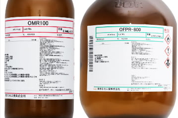
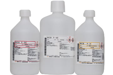
Photoresists,
a chemical essential for semiconductor manufacturing.
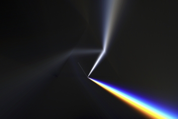
The photoresists known as a photosensitive material, initiate a chemical reaction in the light.
It is a chemical that plays an essential role in photolithography, a technology that is involved in
the manufacture of semiconductor devices.
In the semiconductor manufacturing, the exposure process that a photoengraving technique is applied
to reduce and transfer the design drawn on the original plate (photomask) onto the silicon chip.
To create power-saving, high-performance semiconductors,
the circuits that are to be transferred need to be rendered smaller.
Our photoresists are evolving from one day to the next in order to satisfy this requirement.
TOK has the top share of the global market
for semiconductor photoresists.*1
In 1968, TOK began developing and selling the first made-in-Japan semiconductor photoresists.
These days, we offer a full lineup of photoresists compatible with all exposure machines and are highly competitive in the market.
TOK’s market share
for semiconductor photoresists
(based on projected shipment volume in 2022*2)
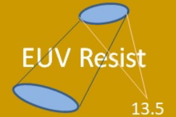
EUV
photoresists
ArF excimer laser
photoresists
KrF excimer laser
photoresists
g/i-Line
photoresists
TOK’s Products in Semiconductor Manufacturing Field

Core Technology
The world leading micro-fabrication and high purification technologies
Our products, which are used to semiconductor manufacturing featuring cutting-edge circuits produced at a scale of several nanometers, are supported by two global-leading core technologies.
