Semiconductor Packaging Manufacturing Field
The process of separating the wafer into individual semiconductor chips, and place them into protective package. Photoresists and other chemicals provided by TOK are also used in this area.
Semiconductor manufacturing flow
Packaging Process
- Photoresist coating
- Exposure
- Development
- Plating process
- Photoresist cleaning
- Coating on the back
- Dicing
- Molding
- Photoresist coating
- Exposure
- Development
- Plating process
- Photoresist cleaning
- Coating on the back
- Dicing
- Molding
Process.15Photoresist coating
Apply a photoresist to the silicon substrate after the completion of the upstream process.
Process.16Exposure
Circuit design of photomask is transferred to coated photoresist film by irradiation of light.
Process.17Development
The photoresist pattern is formed by development.
Process.18Plating process
Using the resist pattern as a mold, form connector on pillars known as BUMPs.
Process.19Photoresist cleaning
Use a cleaning solution to remove any photoresist that is no longer needed.
Process.20Coating on the back
Coat the backside of the silicon substrate with the sealant.
Process.21Dicing
Wafer is diced into chipsize components.
Process.22Molding
Set and fix cut-out semiconductor chips onto a substrate
Packaging technology to render semiconductor
chips smaller, thinner, and capable of delivering higher performance
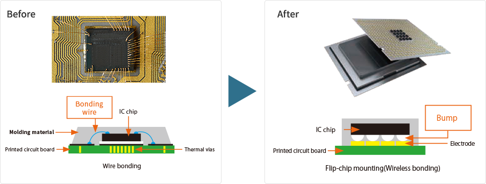
Flip-chip mounting
(Wireless bonding)
The finished semiconductor chip needs to be powered on by having it make contact with the substrate.
This used to be typically done by connecting the chip
to the frame using thin metal wires according to a method known as wire bonding.
These days, however, flip-chip mounting,
which entails the use of protruding connection terminals (bumps) instead of wires,
is predominantly used in this field.
Connecting semiconductor chips to substrates: the changing face of technology
We are helping to make semiconductor packages smaller and capable of delivering higher performance.
TOK’s Products in Semiconductor Packaging Manufacturing Field


Core Technology
The world leading micro-fabrication and high purification technologies
Our products, which are used to semiconductor manufacturing featuring cutting-edge circuits produced at a scale of several nanometers, are supported by two global-leading core technologies.
